
Solid State Drives (SSDs) have taken the computer industry by storm in recent years. The technology is impressive with its high-speed capabilities. It promises low-latency access to sometimes critical data while increasing overall performance, at least when compared to what is now becoming the legacy Hard Disk Drive (HDD). With each passing year, SSD market shares continue to climb, replacing the HDD in many sectors. The effects of this are seen in personal, mobile and server computing.
IBM first unleashed the HDD into the computing world in 1956. By the 1960s, the HDD became the dominant secondary storage device for general-purpose computers (emphasis on secondary storage device, memory being the first). Capacity and performance were the primary characteristics defining the HDD. In many ways, those characteristics continue to define the technology—although, not in the most positive ways (more details on that shortly).
The first IBM-manufactured hard drive, the 350 RAMAC, was as large as two medium-sized refrigerators with a total capacity of 3.75MB on a stack of 50 disks. Modern HDD technology has produced disk drives with volumes as high as 16TB, specifically with the more recent Shingled Magnetic Recording (SMR) technology coupled with helium—yes, that's the same chemical element abbreviated as He in the periodic table. The sealed helium gas increases the potential speed of the drive while creating less drag and turbulence. Being less dense than air, it also allows more platters to be stacked in the same space used by 2.5" and 3.5" conventional disk drives.
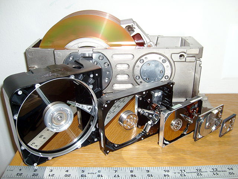
Figure 1. A lineup of Standard HDDs throughout Their History and across All Form Factors (by Paul R. Potts—Provided by Author, CC BY-SA 3.0 us, https://commons.wikimedia.org/w/index.php?curid=4676174)
A disk drive's performance typically is calculated by the time required to move the drive's heads to a specific track or cylinder and the time it takes for the requested sector to move under the head—that is, the latency. Performance is also measured at the rate by which the data is transmitted.
Being a mechanical device, an HDD does not perform nearly as fast as memory. A lot of moving components add to latency times and decrease the overall speed by which you can access data (for both read and write operations).
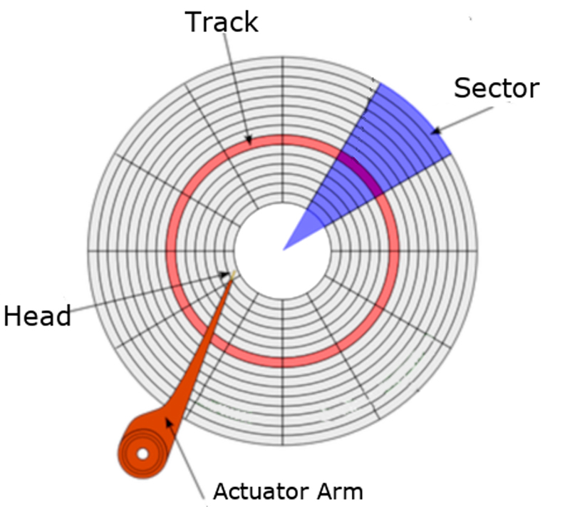
Figure 2. Disk Platter Layout
Each HDD has magnetic platters inside, which often are referred to as disks. Those platters are what stores the information. Bound by a spindle and spinning them in unison, an HDD will have more than one platter sitting on top of each other with a minimum amount of space in between.
Similar to how a phonograph record works, the platters are double-sided, and the surface of each has circular etchings called tracks. Each track is made up of sectors. The number of sectors on each track increases as you get closer to the edge of a platter. Nowadays, you'll find that the physical size of a sector is either 512 bytes or 4 Kilobytes (4096 bytes). In the programming world, a sector typically equates to a disk block.
The speed at which a disk spins affects the rate at which information can be read. This is defined as a disk's rotation rate, and it's measured at revolutions per minute (RPM). This is why you'll find modern drives operating at speeds like 7200 RPM (or 120 rotations per second). Older drives spin at slower rates. High-end drives may spin at higher rates. This limitation creates a bottleneck.
An actuator arm sits on top of or below a platter. It extends and retracts over its surface. At the end of the arm is a read-write head. It sits at a microscopic distance above the surface of the platter. As the disk rotates, the head can access information on the current track (without moving). However, if the head needs to move to the next track or to an entirely different track, the time to read or write data is increased. From a programmer's perspective, this is referred to as the disk seek, and this creates a second bottleneck for the technology.
Now, although HDDs' performance has been increasing with newer disk access protocols—such as Serial ATA (SATA) and Serial Attached SCSI (SAS)—and technologies, it's still a bottleneck to the CPU and, in turn, to the overall computer system. Each disk protocol has its own hard limits on maximum throughput (megabytes or gigabytes per second). The method in which data is transferred is also very serialized. This works well with a spinning disk, but it doesn't scale well to Flash technologies.
Since its conception, engineers have been devising newer and more creative methods to help accelerate the HDDs' performance (for example, with memory caching), and in some cases, they've completely replaced them with technologies like the SSD. Today, SSDs are being deployed everywhere—or so it seems. Cost per gigabyte is decreasing, and the price gap is narrowing between Flash and traditional spinning rust. But, how did we get here in the first place? The SSD wasn't an overnight success. Its history is more of a gradual one, dating back as far as when the earliest computers were being developed.
Memory comes in many forms, but before Non-Volatile Memory (NVM) came into the picture, the computing world first was introduced to volatile memory in the form of Random Access Memory (RAM). RAM introduced the ability to write/read data to/from any location of the storage medium in the same amount of time. The often random physical location of a particular set of data did not affect the speed at which the operation completed. The use of this type of memory masked the pain of accessing data from the exponentially slower HDD, by caching data read often or staging data that needed to be written.
The most notable of RAM technologies is Dynamic Random Access Memory (DRAM). It also came out of the IBM labs, in 1966, a decade after the HDD. Being that much closer to the CPU and also not having to deal with mechanical components (that is, the HDD), DRAM performed at stellar speeds. Even today, many data storage technologies strive to perform at the speeds of DRAM. But, there was a drawback, as I emphasized above: the technology was volatile, and as soon as the capacitor-driven integrated circuits (ICs) were deprived of power, the data disappeared along with it.
Another set of drawbacks to the DRAM technology is its very low capacities and the price per gigabyte. Even by today's standards, DRAM is just too expensive when compared to the slower HDDs and SSDs.
Shortly after DRAM's debut came Erasable Programmable Read-Only Memory (EPROM). Invented by Intel, it hit the scene at around 1971. Unlike its volatile counterparts, EPROM offered an extremely sought-out industry game-changer: memory that retains its data as soon as system power is shut off. EPROM used transistors instead of capacitors in its ICs. Those transistors were capable of maintaining state, even after the electricity was cut.
As the name implies, the EPROM was in its own class of Read-Only Memory (ROM). Data typically was pre-programmed into those chips using special devices or tools, and when in production, it had a single purpose: to be read from at high speeds. As a result of this design, EPROM immediately became popular in both embedded and BIOS applications, the latter of which stored vendor-specific details and configurations.
As time progressed, it became painfully obvious: the closer you move data (storage) to the CPU, the faster you're able to access (and manipulate) it. The closest memory to the CPU is the processor's registers. The amount of available registers to a processor varies by architecture. The register's purpose is to hold a small amount of data intended for fast storage. Without a doubt, these registers are the fastest way to access small sizes of data.
Next in line, and following the CPU's registers, is the CPU cache. This is a hardware cache built in to the processor module and utilized by the CPU to reduce the cost and time it takes to access data from the main memory (DRAM). It's designed around Static Random Access Memory (SRAM) technology, which also is a type of volatile memory. Like a typical cache, the purpose of this CPU cache is to store copies of data from the most frequently used main memory locations. On modern CPU architectures, multiple and different independent caches exist (and some of those caches even are split). They are organized in a hierarchy of cache levels: Level 1 (L1), Level 2 (L2), Level 3 (L3) and so on. The larger the processor, the more the cache levels, and the higher the level, the more memory it can store (that is, from KB to MB). On the downside, the higher the level, the farther its location is from the main CPU. Although mostly unnoticeable to modern applications, it does introduce latency.
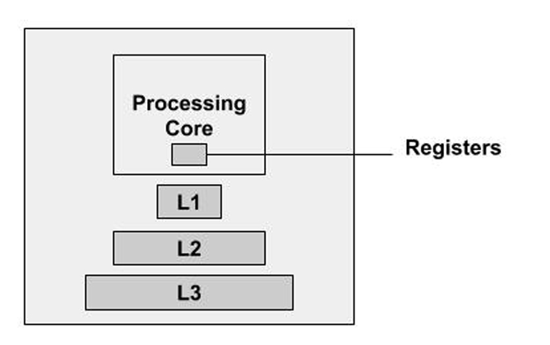
Figure 3. General Outline of the CPU and Its Memory Locations/Caches
The first documented use of a data cache built in to the processor dates back to 1969 and the IBM System/360 Model 85 mainframe computing system. It wasn't until the 1980s that the more mainstream microprocessors started incorporating their own CPU caches. Part of that delay was driven by cost. Much like it is today, (all types of) RAM was very expensive.
So, the data access model goes like this: the farther you move away from the CPU, the higher the latency. DRAM sits much closer to the CPU than an HDD, but not as close as the registers or levels of caches designed into the IC.
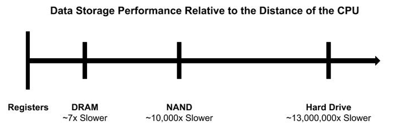
Figure 4. High-Level Model of Data Access
The performance of a given storage technology was constantly gauged and compared to the speeds of CPU memory. So, when the first commercial SSDs hit the market, it didn't take very long for both companies and individuals to adopt the technology. Even with a higher price tag, when compared to HDDs, people were able to justify the expense. Time is money, and if access to the drives saves time, it potentially can increase profits. However, it's unfortunate that with the introduction of the first commercial NAND-based SSDs, the drive didn't move data storage any closer to the CPU. This is because early vendors chose to adopt existing disk interface protocols, such as SATA and SAS. That decision did encourage consumer adoption, but again, it limited overall throughput.
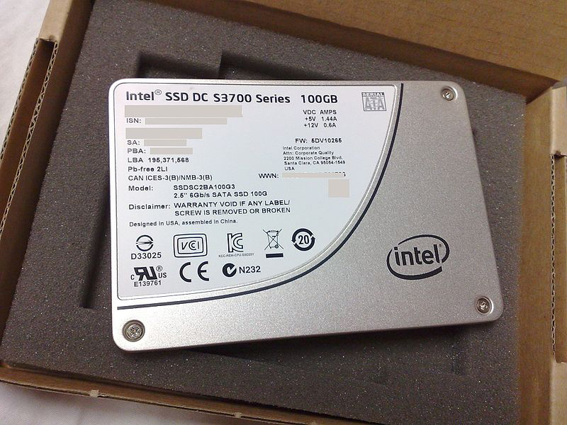
Figure 5. SATA SSD in a 2.5" Drive Form Factor
Even though the SSD didn't move any closer to the CPU, it did achieve a new milestone in this technology—it reduced seek times across the storage media, resulting in significantly less latencies. That's because the drives were designed around ICs, and they contained no movable components. Overall performance was night and day compared to traditional HDDs.
The first official SSD manufactured without the need of a power source (that is, a battery) to maintain state was introduced in 1995 by M-Systems. They were designed to replace HDDs in mission-critical military and aerospace applications. By 1999, Flash-based technology was designed and offered in the traditional 3.5" storage drive form factor, and it continued to be developed this way until 2007 when a newly started and revolutionary startup company named Fusion-io (now part of Western Digital) decided to change the performance-limiting form factor of traditional storage drives and throw the technology directly onto the PCI Express (PCIe) bus. This approach removed many unnecessary communication protocols and subsystems. The design also moved a bit closer to the CPU and produced a noticeable performance improvement. This new design not only changed the technology for years to come, but it also even brought the SSD into traditional data centers.
Fusion-io's products later inspired other memory and storage companies to bring somewhat similar technologies to the Dual In-line Memory Module (DIMM) form factor, which plugs in directly to the traditional RAM slot of the supported motherboard. These types of modules register to the CPU as a different class of memory and remain in a somewhat protected mode. Translation: the main system and, in turn, the operating system did not touch these memory devices unless it was done through a specifically designed device driver or application interface.
It's also worth noting here that the transistor-based NAND Flash technology still paled in comparison to DRAM performance. I'm talking about microsecond latencies versus DRAM's nanosecond latencies. Even in a DIMM form factor, the NAND-based modules just don't perform as well as the DRAM modules.
What makes an SSD faster than a traditional HDD? The simple answer is that it is memory built with chips and no moving components. The name of the technology—solid state—captures this very trait. But if you'd like a more descriptive answer, keep reading.
Instead of saving data onto spinning disks, SSDs save that same data to a pool of NAND flash. The NAND (or NOT-AND) technology is made up of floating gate transistors, and unlike the transistor designs used in DRAM (which must be refreshed multiple times per second), NAND is capable of retaining its charge state, even when power is not supplied to the device—hence the non-volatility of the technology.
At a much lower level, in a NAND configuration, electrons are stored in the floating gate. Opposite of how you read boolean logic, a charge is signified as a "0", and a not-charge is a "1". These bits are stored in a cell. It is organized in a grid layout referred to as a block. Each individual row of the grid is called a page, with page sizes typically set to 4K (or more). Traditionally, there are 128–256 pages per block, with block sizes reaching as high as 1MB or larger.
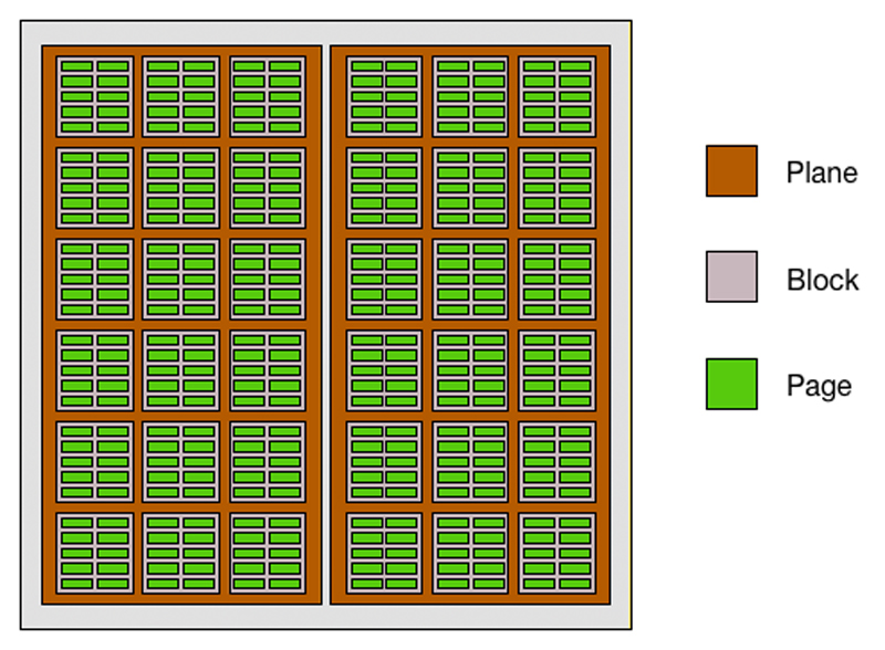
Figure 6. NAND Die Layout
There are different types of NAND, all defined by the number of bits per cell. As the name implies, a single-level cell (SLC) stores one bit. A multi-level cell stores two bits. Triple-level cells store three bits. And, new to the scene is the QLC. Guess how many bits it can store? You guessed it: four.
Now, although a TLC offers more storage density than an SLC NAND, it comes at a price: increased latency—that is, approximately four times worse for reads and six times worse for writes. The reason for this rests on how data moves in and out of the NAND cell. In an SLC NAND, the device's controller needs to know only if the bit is a 0 or a 1. With an MLC, the cell holds more values—four to be exact: 00, 01, 10 or 11. In a TLC NAND, it holds eight values: 000, 001, 010, 011, 100, 101, 110, 111. That's a lot of overhead and extra processing. Either way, regardless of whether your drive is using SLC or TLC NAND, it still will perform night-and-day faster than an HDD—minor details.
There's a lot more to share about NAND, such as how reads, writes and erases (Programmable Erase or PE cycles) work, the last of which does eventually impact write performance and some of the technology's early pitfalls, but I won't bore you with that. Just remember: electrical charges to chips are much faster than moving heads across disk platters. It's time to introduce the NVMe.
Okay, I lied. Write performance can and will vary throughout the life of the SSD. When an SSD is new, all of its data blocks are erased and presented as new. Incoming data is written directly to the NAND. Once the SSD has filled all of the free data blocks on the device, it then must erase previously programmed blocks to write the new data. In the industry, this moment is known as the device's write cliff. To free the old blocks, the chosen blocks must be erased. This action is called the Programmable Erase (PE) cycle, and it increases the device's write latency. Given enough time, you'll notice that a used SSD eventually doesn't perform as well as a brand-new SSD. A NAND cell is programmed to handle a finite amount of erases.
To overcome all of these limitations and eventual bottlenecks, vendors resort to various tricks, including the following:
Fusion-io built a closed and proprietary product. This fact alone brought many industry leaders together to define a new standard to compete against the pioneer and push more PCIe-connected Flash into the data center. With the first industry specifications announced in 2011, NVMe quickly rose to the forefront of SSD technologies. Remember, historically, SSDs were built on top of SATA and SAS buses. Those interfaces worked well for the maturing Flash memory technology, but with all the protocol overhead and bus speed limitations, it didn't take long for those drives to experience their own fair share of performance bottlenecks (and limitations). Today, modern SAS drives operate at 12Gbit/s, while modern SATA drives operate at 6Gbit/s. This is why the technology shifted its focus to PCIe. With the bus closer to the CPU, and PCIe capable of performing at increasingly stellar speeds, SSDs seemed to fit right in. Using PCIe 3.0, modern drives can achieve speeds as high as 40Gbit/s. Support for NVMe drives was integrated into the Linux 3.3 mainline kernel (2012).
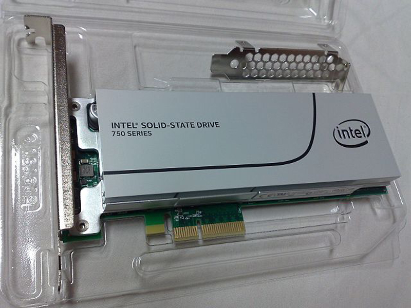
Figure 7. A PCIe NVMe SSD (by Dsimic - Own work, CC BY-SA 4.0, https://commons.wikimedia.org/w/index.php?curid=41576100)
What really makes NVMe shine over the operating system's legacy storage stacks is its simpler and faster queueing mechanisms. These are called the Submission Queues (SQs) and Completion Queues (CQs). Each queue is a circular buffer of a fixed size that the operating system uses to submit one or more commands to the NVMe controller. One or more of these queues also can be pinned to specific cores, which allows for more uninterrupted operations. Goodbye serial communication. Drive I/O is now parallelized.
In the world of SAS or SATA, there is the Storage Area Network (SAN). SANs are designed around SCSI standards. The primary goal of a SAN (or any other storage network) is to provide access of one or more storage volumes across one or more paths to a single or multiple operating system host(s) in a network. Today, the most commonly deployed SAN is based on iSCSI, which is SCSI over TCP/IP. Technically, NVMe drives can be configured within a SAN environment, although the protocol overhead introduces latencies that make it a less than ideal implementation. In 2014, the NVMe Express committee was poised to rectify this with the NVMeoF standard.
The goals behind NVMeoF are simple: enable an NVMe transport bridge, which is built around the NVMe queuing architecture, and avoid any and all protocol translation overhead other than the supported NVMe commands (end to end). With such a design, network latencies noticeably drop (less than 200ns). This design relies on the use of PCIe switches. A second design has been gaining ground that's based on the existing Ethernet fabrics using Remote Direct Memory Access (RDMA).
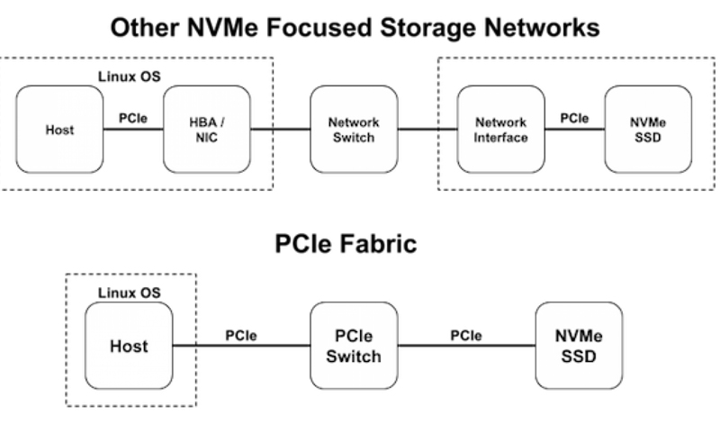
Figure 8. A Comparison of NVMe Fabrics over Other Storage Networks
The 4.8 Linux kernel introduced a lot of new code to support NVMeoF. The patches were submitted as part of a joint effort by the hard-working developers over at Intel, Samsung and elsewhere. Three major components were patched into the kernel, including the general NVMe Target Support framework. This framework enables block devices to be exported from the Linux kernel using the NVMe protocol. Dependent upon this framework, there is now support for NVMe loopback devices and also NVMe over Fabrics RDMA Targets. If you recall, this last piece is one of the two more common NVMeoF deployments.
So, there you have it, an introduction and deep dive into Flash storage. Now you should understand why the technology is both increasing in popularity and the preferred choice for high-speed computing. Part II of this article shifts focus to using NVMe drives in a Linux environment and accessing those same NVMe drives across an NVMeoF network.
Petros Koutoupis, LJ Editor at Large, is currently a senior platform architect at IBM for its Cloud Object Storage division (formerly Cleversafe). He is also the creator and maintainer of the RapidDisk Project. Petros has worked in the data storage industry for well over a decade and has helped pioneer the many technologies unleashed in the wild today.
